P235
Circuit Board Artwork and Construction
Not all radio amateurs want or need to build a printed circuit board. Many who follow the hobby for some time will encounter a reason to give it a try. The task has a pretty steep learning curve.
On this page we examine what is really important and what is often touted as important, but isn’t. it’s a reflection of personal experience. Others may have a different perspective on the topic. This information does not specify any particular software package.
The full article appeared in the QTC magazine in November 2024 and can be found here:
https://vkradioamateurs.org/home/qtc-magazine/qtc-pdf-download/
or via the flip magazine: https://qtcmag.com/books/ectx/#p=12
Etch your own PCB’s?
My advice is “don’t do it”. Your design time is valuable and the results will be ordinary. It won’t have protective green solder mask, it probably won’t be double-sided, won’t have a printed component legend and won’t have plated-through holes. Today, the tooling and chemicals you need to do this are going to cost more than the price of many manufactured boards.
Focus on your design, get your CAD file as good as you can and email your files to a specialist pcb maker. Two weeks later you will have some nice pcb’s arriving in your letter box, far better than anything you can produce at home.
Don’t bother veroboarding a full prototype of your project.
Many project builders will try to create their entire project as a rough prototype on veroboard, or other copper strip panels, before going to pcb artwork. This is very slow, can introduce many errors on a layout that is going to be discarded anyway. It is no fun trying to debug a rough version where components and values are not labelled. Certainly, if you want to advance-check a small aspect such as ideal op-amp or voltage regulator values on a breadboard, do that. Once proven and the circuit has been confirmed, put it aside.

Document your schematic circuit on paper or on screen as good as accurate as you can make it, then go straight to a version 1 circuit board layout. When you get the board back and build up a proper Version 1, it will be much easier to test and trial this than wrestling with a lash-up job. If the project has software in it, you will want to know how it behaves on a board much closer to that which you intend to use. Ultimately, it is faster and cheaper than struggling to commission a half-assed version of the design. This leads us to the next topic:
Version 1 of any board will probably have issues.
When preparing circuit board artwork it is ok to get your layout as good as you can before sending it off for production. However, when you get it back and put it together for the first time, you will usually find some unexpected surprises. Maybe the parts that you thought would fit, don’t fit, or they conceal legend text. Mounting wires could be thicker than the holes size you had chosen. Perhaps there were alignment or physical collisions in the enclosure you selected. The point is that as much as you would like the board to be perfect, there will be changes. Accept this and learn from it. Immediately save your layout as v2 and make edits to it as you go, even if you never get proceed to a v2 in production.
Put a date on your Circuit board?
The circuit board should have the project code and version somewhere on the component overlay. Where sufficient room exists, adding the Year and Month of the design can be helpful. This is not essential, but it does tie the new design to a creation date. Handy in years to come.
Schematic diagrams
It is good practise to start the layout with a quality schematic drawing. Perhaps you have made a hand-drawn diagram and are keen to get into the board layout. Take the time to draw a proper schematic on an A4 sized page using the PCB schematic package. Ensure that every component has a part number (R1, R2, C1 etc.) You will have to make a good diagram anyway, so do it first.
Netlists
A Netlist is a list of connections that can be created by your schematic editor, detailing as a list of every component that is electrically connected together to other components or terminals. The theory is that a Netlist can later be reconciled against your circuit board layout and the program can alert you if some connections were left off the board. The principle is good and some designers swear by it. Others swear at it.
My personal choice is not to use net lists as there can be a lot of work to get it right, particularly where your design has a lot of special parts in it. I print a fresh copy of the schematic and as a track is placed on the board layout, I highlight that connection with a fluro marking pen on the schematic diagram. Then keep going until every line on the diagram has been coloured in.
Set your board size
This is a bit of an art. Place most of your parts on a bit of paper, Push them around until the parts that will be electrically near each other on the circuit are close on the paper, with enough room for a few tracks to run between them. Where possible, orient all the IC’s so that Pin 1 is towards the top of the board.
If size is not critical, be generous with the parts spacing. The art comes into it when you decide what sized enclosure you are going to put the board into. Make the enclosure no bigger than necessary, but don’t go for too compact if you don’t have to. Small boards are harder to design than big boards.
Selecting the enclosure first is really important. Good enclosures have circuit board mounts of defined spacing. Make your circuit board outline fit the enclosure, not the other way around, or you will finish up with a board that does not quite fit in many boxes, but rattles around in one that is much bigger than it ought to be.
Grid selection – Metric vs Imperial
Many beginners get this wrong. Most of the components are still manufactured on an imperial grid. Dual-in-line IC’s and connector headers are usually based upon 0.1 inch spacing. Pads between pigtailed ¼ watt resistors are normally 0.4 inches apart. Capacitors are 0.1 or 0.2 inch pitch. However, larger parts and the mounting screws on enclosures will all be in Metric. So here’s the trick. Start with your CAD package set to a Metric grid. Probably 0.5 mm per step. Draw a line using one of the mechanical layers (not a track but a line) to outline the perimeter of the board. Still on the metric grid, Place large pads where the screws are going to mount at the four (or 6) mounting points of the enclosure.
Once this is done, set your cursor to the Bottom Left hand corner of the board and define this corner as your Point of Origin. Don’t place ANY components on the layout yet.
Now it is safe to switch your CAD package to an imperial grid and set the step rate to 25mil. One mil is one-thousandth of an inch. With 25 mil steps, each pin of an IC will be exactly four steps apart on your layout. Use the Imperial grid for the rest of your design. (Later, when tidying up, it is ok to set the step to 5 mil when it comes to aesthetically moving component text to exactly where you want it to be.)
While safely on the 25 mil imperial grid, place all of your components on the board and roughly move them around to where you think they aught to be. Later they may have to be adjusted as the board layout progresses, but it is a good start.
Putting your layout together
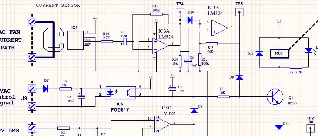
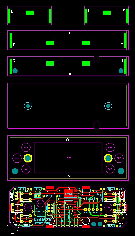
In the example below there is a simple design for a hand held remote control on 433.920 MHz. It is used for fox hunts and clock adjustments, but that’s not important right now. The artwork is here to serve as an example for several design aspects.

A simple 2-layer board as viewed on a CAD package
Selection of Colours
CAD packages let designers choose their artwork colours. There are some conventions, but this is unimportant. Pick whatever works for you. Go for high contrast and colours that will still work if you choose to make a colour print of the layout with a laser printer.
Another personal choice is the background colour. (I prefer to work on a plain black background.) This table details the colours used in the above example board:
| GREEN | Top Layer | Tracks on the top of the board. (on a double-sided board) |
| RED | Bottom Layer | Tracks on the underside of the board. |
| YELLOW | Multi-Layer | Pads etc that appear on both sides of the board. |
| BLUE | Holes | This denotes the holes that will be drilled in the board. |
| WHITE | Top Legend | Normally printed in white paint, this is your component. |
| PALE BLUE | Bottom Legend | Seldom used but if parts get mounted on the bottom of the board, this will be for the component identification. |
| VIOLET | Mech Layer #1 | This is a line, not a track. It is used to define the outline of the design and any large holes to be cutout. |
Component positioning & Text
All resistors, inductors and IC’s have their value written under the part to assist with placement during construction and the part designation next to the component. They are well spaced. It helps if all diodes can be oriented the same way. Again for ease of placement and it sticks out if one was put in backwards when troubleshooting. If you don’t have the footprint of the part you need, create one and save it to your library of favourite parts. How this is done varies somewhat between CAD applications. Don’t trust parts libraries until you have physically compared the virtual part with the real part. Lots of component libraries have hole size and clearance errors. A digital vernier is an essential tool during this time.
Remember if you are doing a board with a component legend or writing on both sides of a board, that the text on the lower side is always mirrored during your layout. If both sides are readable during your design phase, then one side is going to look pretty stupid when you get your pcb back from the maker.
Note that a small square white square has been manually placed near Pin 1 of all IC’s. This is optional but good practice so as to leave no doubt which way the chip goes on the board. The part outline shows this orientation, but it can also be obscured by IC sockets.
Think about what will make the board tough in the field. This board was powered by a 9V battery. In the bottom left there are two pads labelled + and – used for the battery clip on two wires. These wires will break off with very little flexing, so two holes have been placed next to the pads for the wires to thread through for strain relief. Larger cables directly connecting to a board should have two 4mm holes for supporting a small cable tie. It is attention to these little things which improves the reliability of the final product.
Track widths
There is a temptation to make tracks very thin, 10 mil or less, because they look good on the screen during design time. Get into the habit of making tracks as thick as the board will easily support. It makes the design tougher. In this example, which had a surface mount microprocessor, most tracks were 20 mil wide. Generally I make power rails (0V, +5V, +12V) wider at 50 or 100 mil, depending upon current demands. If I had to run a track between legs of a DIP ic, I would make the adjacent pads oval shaped and reduce that part of the track to 15 mil. Sure you can design your board with 5 mil tracks and get away with it. The pcb company will make it for you and maybe it would be ok. Unless there is no alternative, don’t do it. Very thin tracks will make your final design unnecessarily fragile.
Component pad & hole sizes
Pads are what anchor your part to the board. Mostly resistors and small capacitor pads should be 65 or 70 mil in diameter, with a 32 mil hole. Diodes often have thicker leads and need bigger holes, so diode footprints have at least 70 mil pads and 40 mil holes (40 mil is about 1 mm). Headers for IDC connectors and programming ports also need 70 mil pads and 40 mil holes. I prefer DIP IC footprints to have round pads, leaving more space for tracks under the IC’s. If you want a clean screw hole of say 3.5mm for a 3mm screw to pass through, it is ok to place a pad on the artwork and set the hole size to be larger than the pad.
Go easy on the cornering…
Don’t put down tracks that turn corners at 90 degrees. It looks weird and is not the most compact way for laying down tracks. Take another look at the above sample board and you will see that all tracks turn in 45 degree steps. Much better. It improves track density. On double sided boards, ensure that tracks on the top layer don’t go too close to holes for mounting screws. You don’t want screw heads coming down on tracks where they can cut tracks or short them to a chassis.
Single or Double sided PCB’s?
In the dark, early days, single sided boards with copper only on the underside of a layout were much cheaper than double sided boards. Today the price difference is not great, as the majority of circuit boards are now double sided. Plan on making all of your designs to be Double Sided boards.
There is another reason for Double sided boards. On Single Sided pcb’s, parts pass through the board and solder to pads on the underside. The only thing keeping the pad in place is the glue between the copper and the fibreglass. Any vibration on the board, or brief impact to say a capacitor, can cause the pad to lift and shear away from the track that feeds it. Suddenly your project is intermittent and unstable.
Where the board is Double Sided, the interior of the hole is lined with a copper sleeve. That is your Plated Through Hole or ‘PTH’ in industry jargon. When PTH pads are soldered, the solder soaks through the hole and anchors to the pad on the top side of the board. This is much stronger. Double Sided boards are always going to be significantly tougher than single sided boards. I made plenty of modules for early golf cart electronics and saw what came back over time. (particularly if they hit their electronics with a club after a bad shot) Board integrity failures fell to zero after a transition to double sided boards was made. Today, even if I were making a design with no tracks on the top of the board, I would still order it as a double sided board with plated through holes. The small price difference for the avoidance of future failure is money well spent.
High Voltage vs Low Voltage areas
Perhaps your design has a small power transformer on it with a 240V primary, or a relay which will switch 240V. You will want to keep all mains powered tracks at least 10mm away from your low voltage circuitry. I like to place a wide track or fill 10mm wide and put it on the layer which is a Solder Mask Void layer. This path will go between the high and low voltage zones on the board and make it clear to anyone working with the module that compliant isolation is present.
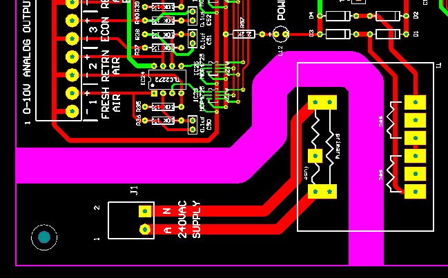
A clearly defined 10mm high voltage safety barrier in the lower solder mask
Auto-Route?
Auto-routing of board layouts have been around for a long time and it has gotten pretty good. With this technology, you put down your parts, highlight pads to be connected and let the program draw your tracks for you. Try it if you like. Personally, I don’t use this feature. I prefer to manually insert my tracks. It forces me to think harder about component placement. For auto-routing to work properly, design rules and net lists have to be spot on. This also takes time. After auto-routing, some corrections and human interventions is still going to be necessary in complex areas of a layout. (Like cars, driving an auto is fine, but if you really want to understand what your car is doing, drive Manual first.)
PCB board & copper thickness
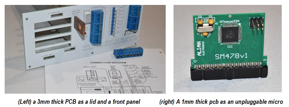
The standard thickness for a fibreglass circuit board is 1.6 mm thick and the copper is 35 microns thick. This is fine for 95% of jobs. There have been times when I have ordered boards to be 1mm thick, so that it can fit on to IDC header plugs. (shown below) There have been projects where the circuit board had been part of the structure where it was ordered as a tough 3mm thick board, as with this forklift motor controller. We can afford to be creative with this work. The forklift unit had a 3mm pcb lid with zero trackwork, holes pre-drilled, white solder mask and customer wiring diagram printed on top.
There will be some occasions where high current flow is a factor. In some golf cart pcb’s, wide tracks on top and bottom of a board are run in parallel to double the current capacity. Optionally, the pcb can be ordered with copper 70 microns thick instead of the usual 35, which will double the current capacity again. These are all possibilities.
Multi layer boards?
Most big pcb companies offer multi-layer boards where there are extra copper layers between top and bottom layers. This can increase the component density of a board, or offer a shielding layer to RF sensitive boards. I do not usually design such boards. They do get expensive. Should something happen to a track in a buried layer, the board cannot be serviced. By all means try it, but stick to double sided boards wherever you can.
Solder mask & component legend colours
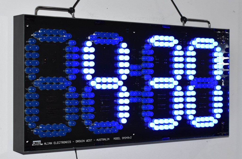
When ordering your circuit boards you will be asked to nominate a solder mask colour and a component legend colour. The default colours are pretty much white text on a green protective solder mask. That’s fine. Mostly people won’t see it anyway. Sometimes it’s nice to do something special and go for white writing on a black solder mask, like this blue LED clock assembled for the next Antennapalooza event. The side panels of the clock which hold the acrylic screen are also pcb material. In the right situation black text on a white solder mask can also be very effective.
PCB’s as building materials
As seen in the previous section, it is quit feasible to use circuit board as an enclosure construction material. You get something that is tougher and more UV stable than 3-D printed plastics. Certainly it is a lot cheaper than getting dies made for injection moulded plastics. In this example the pcb layout can include multiple panels of the enclosure, with all holes and cutouts prepared in the layout, plus the circuit board itself that sits in the centre of the enclosure.
There are copper fill areas on the ends of each panel allowing the enclosure to be assembled by solder deposits on the inside. The edges of the front and rear panels have had the first 1.6 mm routed down 1, deep, so that when the enclosure is screwed together, the corners of the box come together neatly.
The front and rear panels clamshell together with 3mm screws. Push button switches come up flush with the front surface so that the label will flex when a button is pressed. The two holes in the base of the enclosure were for photocells to dim the OLED display at night. Sure you have to put it together, but this is still faster, neater and more repeatable than drilling a bunch of holes yourself in a plastic box.
If the edges of front and rear panels are machined, you get a neat box

Pre-order integrity checks
If you have completed the pcb layout and you think it’s about right, then there’s another step that may save your project from tragedy. On the screen, turn off the component legend layer and the top copper layer. Now you should see the bottom layer tracks and pads in the clear. Carefully inspect the board. Are clearances to pads and other tracks good? Could some tracks be centred a little better? Did you lay a track around something that is no longer there? Maybe it’s ok to make a track take a more direct path on this layer. Did a track pass through a hole or cutout? Such issues are reasonably easy to spot with this view.
Next turn off the bottom layer, turn on the Top copper layer and repeat the exercise. When that is done, turn both copper layers off and activate the component legend to see how the text is going to look on the board. For this layer, I set the layout grid to just 5 mil, so that I can more accurately position the text next to the parts. Ensure that the text is not on top of any vias or pads, as that text will be lost. Ensure that all the screw terminals are correctly labelled. Add any other relevant text if there is room, such as what option links do when they are in or out. When all this is done you are ready to send your file to a pcb maker.
Pick a pcb company
There used to be many circuit board manufacturing companies in Australia. The quality was good, but they were slow. One by one they disappeared. Tooling and production costs were very high. I patronised Australian manufacturers for as long as I could, then discovered that some companies were just taking my orders, quietly getting the boards made in China anyway and charging an extra 100% for the handling.
When ready, email the pcb file, along with my requirements Within another couple of hours they do a technical assessment and ask questions if there are anomalies spotted by the production team. A track that goes nowhere? (Yes that’s supposed to be an antenna track) Should these holes be plated through? Sure why not. The written email English by the staff in these companies is quite good and they have been universally supportive.
Within 5 days the job will be done, whether it is 3 or 300 circuit boards. There will be a Tooling fee, a price-per-board fee and a delivery fee. Delivery time is typically 5-10 days later. Be aware, if your order is near Chinese New Year or other national holidays, there will be extra delays.
IC Sockets
Contrary to most industry convention, I tend to use IC sockets for all DIP IC’s. There is a cost per socket. Perhaps 20 cents, but you only have to want to change one chip once and the 20 cent socket cost has become a sound investment. (It takes time to remove and re-solder entire IC’s just on spec that it could be a crook device.) If you decide to make a Version 2 of a circuit board, it’s easy to remove and re-use all the socketed chips from your obsolete version 1 board.
Terminal blocks and Wires
Your design will have wires going to or from the board. I don’t like wires that solder directly to circuit boards. Screw terminals that can be unplugged are best. If the board must be removed, swapped or placed in a test harness, it can be unplugged without loosing the positioning of the connecting wires, preventing future faults. Where there is more than one such connector, ensure that they are of different sizes or number of terminals, so they can’t be swapped accidentally. Leave room for identifying text on the function of each terminal, so it can still be easily read when the connector is plugged in
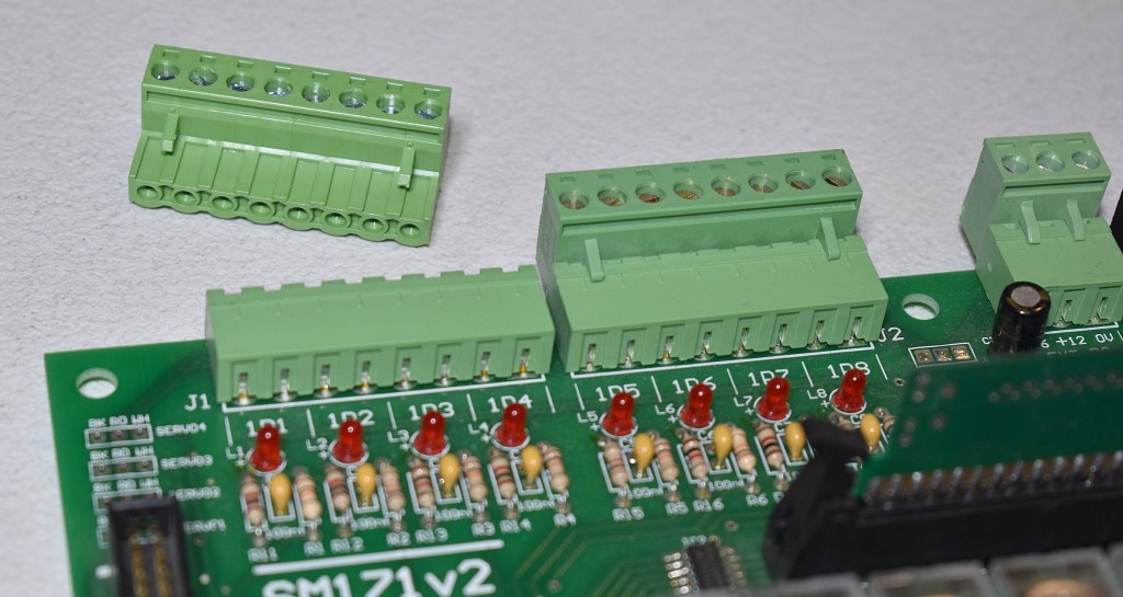
Screw terminal blocks are much nicer than soldered wires
Filling areas with copper
Many designers like to use flood-fill tools to extend a ground plane track work to all parts of the board not occupied by tracks and components. For radio applications, the extra grounding can improve stability. For the rest of the time, the extra ground plane is a distraction and increases the chances of tracks shorting to earth. I don’t often use this feature.
Completing power rail loops
If you have a negative rail, or +5 or +12V power rail traversing your board, try to loop the track ends so that the meet and form a complete circle. It lowers the impedance of the supply and reduces voltage drops on supply rail tracks when they are under load. It’s not always possible, but it can improve stability if you have the track room to do it.
Getting boards cut out, panelised, snap-out or V-grooved
The circuit board maker may ask if you want boards to be joined together in a larger pcb frame that you snap out when ready. The snap areas are either a series of fine holes, or a section that has been partially cut through in the shape of a ‘vee’. Mostly this is harmless and makes them look like they came out of a 1960’s cereal packet. Generally I would request that the boards are fully cut from their supporting frame and are sent ready-to-use, without having to snap them from a frame.
Placing an order
With any new order to a pcb manufacturer, create a one-page Word document that will accompany the artwork file. It should contain the following information:
- PCB filename/version CAT003v2
- An order reference number 1234
- Your contact details, email and delivery address.
- New order or Repeat order (If ‘Repeat’, you don’t need to supply the artwork file)
- The name & version of the pcb package you used to create your layout
- How many boards you want
- Height & width of the board in mm
- PCB thickness Usually 1.6 mm
- Copper thickness Usually 35 um
- Hole quantity Approximation is ok
- Smallest hole size Usually 28 mil in a via hole.
- Thinnest track Check your board. 20 mil is good.
- Layer format Single/Double sided, through hole plated
- Slots or large holes Yes/No
- Layers to ignore
Some mech layers may have been added be there to help you position enclosures and external hardware. The pcb maker should be told to ignore them.
- Solder mask colour Usually green
- Component legend colour Usually white
- Comments Any notes that may help the manufacturer
Clear lacquer?
Many boards will find themselves in a humid, harsh environment, where dirt can get in, ants & spiders nest, or some idiot wants to wash the pcb with a high pressure hose. In those instances, I cover the connectors (and IC sockets if not populated) with masking tape and hit both sides with a clear pressure pack lacquer. The Chemtools ACC400 from Radio Parts is really good for this. Fast drying, clear and easy to solder through if you must do a repair. It does not make a board waterproof, but it does make them last a lot longer in the field.
One extra hole…
Although not part of a circuit board design, consider putting a couple of tiny holes in the bottom of your waterproof enclosures. Remember, nothing holds water better than a waterproof enclosure. I used to make 1mm holes until I encountered a race of 1mm ants. So now I drill 0.7mm holes in boxes.

You want ants? That’s how you get ants
Summing up
This article is already a long one, but contains a lot of information. Perhaps it will help with a single project or maybe it will launch a new career. That’s up to the reader. Like any learned skill, the more boards you design, the better they become.
